
![[a225 11k]](a225.jpg)
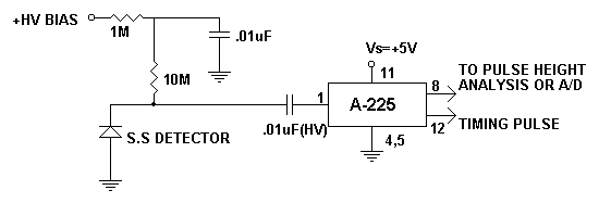
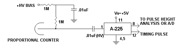
Model A225 is a high performance thin film hybrid charge sensitive preamplifier and shaping amplifier developed especially for high resolution systems employing solid state detectors, proportional counters, photomultiplier tubes and other charge producing detectors in the pulse height analysis or A/D mode of operation.
While these units were specifically designed for satellite instrumentation, the following unique characteristics make them equally useful for space, laboratory and commercial applications:
| Sensitivity | 240 mV/Mev (Si) 300 mV/Mev (Ge) 195 mV/Mev (CdTe) 206 mV/Mev (HgI2) 5.2 x 10 V/coulomb 0.83 µV/electron |
| Noise | 2.5 KeV FWHM (Si) 2.0 KeV FWHM (Ge) 3.1 KeV FWHM (CdTe) 2.9 KeV FWHM (HgI2) 4.5 x 10 coulomb rms 280 electrons rms |
| Noise Slope | 50 eV/pF (Si) 40 eV/pF (Ge) 62 eV/pF (CdTe) 58 eV/pF (HgI2) 9 x 10 coulomb/pF 5.6 electrons/pF |
| Dynamic Input Capacitance | > 7,000 pF |
| Polarity | Negative |
| Detector Capacitance | Up to 1,000 pF |
| Polarity | Positive |
| Peaking Time | 2.4 µs |
| Integral Nonlinearity | < 0.04% for 0 to 10V output pulse |
| Pole-Zero Compensation | Internal |
| Dynamic Range | (Vs - 1.25) Volt |
| DC Level | 0.8 V nominal |
| Polarity | Positive |
| Sensitivity | 44 mV/Mev (Si) 55 mV/Mev (Ge) 1.0 V/picocoulomb |
| Risetime | 18 ns (unloaded) |
| Operating Voltage | Vs = +4 to +25 VDC |
| Operating Current | 2.3 mA independent of Vs |
| Variation of Sensitivity with Supply Voltage | < 0.07% /Volt, 4 to 10 Volts < 0.005% /Volt, 10 to 25 Volts |
| Temperature | -55 to +125 ºC Operational |
| Temperature Stability | 0.02% / ºC at 25 ºC typical ±2% from -25 to +75 ºC |
| Screening | Amptek High Reliability |
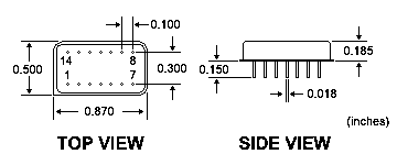
| Package | 14 pin hybrid DIP (metal) |
| Radiation Resistance | 100k rad(Si) |
| Warranty | One year |
| Test Board | PC-25 |
Due to its hermetic seal and small size, the A225 is well suited for use in space or within a vacuum chamber. In such applications care should be taken to avoid electrical discharge near the input which can damage the unit and VOID WARRANTY. Use care in soldering leads - avoid overheating.
For laboratory usage, the A225 can be mounted on its PC-25 test board (see below) and enclosed in a small metal box with appropriate cable connectors. A high voltage coupling capacitor should be added at the input as well as a small hole in the metal box in order to provide screwdriver adjustment to the gain control potentiometer.
| Pin 1 | Input |
| Pin 2 | Case |
| Pin 3 | NC |
| Pin 4 | Input GND and Case |
| Pin 5 | Output GND |
| Pin 6 | NC |
| Pin 7 | NC |
| Pin 8 | Output |
| Pin 9 | Case |
| Pin 10 | NC |
| Pin 11 | Vs = +4 to +25 VDC |
| Pin 12 | Timing Pulse |
| Pin 13 | NC |
| Pin 14 | Compensation (see operating notes below) |
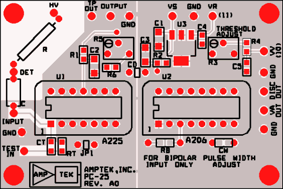
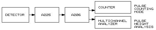
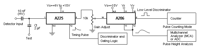
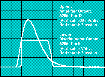
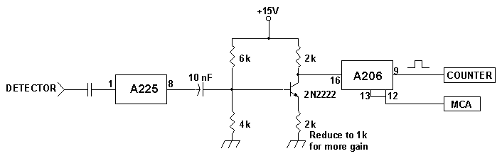
The PC-25 is a printed circuit board which accepts the A225 charge sensitive preamplifier and shaping amplifier and the A206 voltage amplifier and discriminator. It is designed to be used for two purposes: to facilitate testing of these devices, together or separately, and to simplify their use in many applications. The board provides input test circuitry, gain adjustment, voltatge reference to the A206, and convenient access to all active device pins. Ground plane construction minimizes noise pickup.
Due to the high sensitivity and ultra low noise of the A225, care should be taken in circuit layout. The PC-25 Test Board may be used as an example of appropriate layout technique. In general, ground plane construction is recommended. Input and output lines should be kept well separated and in most cases shielding will be necessary. Particular attention should be paid to the detector ground connection to avoid oscillation due to feedback. The supply voltage is internally decoupled. While this is normally adequate, in some applications external bypassing may be helpful.
To facilitate noise minimization in certain applications, two separate ground connections are provided. Pin 4 is the ground connection for the input stage and is also connected to the case. Pin 5 is ground for the remainder of the circuit. In most applications Pin 4 and 5 may be connected to the same ground (preferably a ground plane under the unit) along with Pins 2,3,6,7,9,10 and 13.
The A225 may also be used in applications where the input from the detector is positive by connecting Pin 5 (output ground) to a negative supply voltage instead of ground. This voltage can range from 0 to -10 V. A negative output pulse at Pin 8 will result from a positive input. The dynamic range in this case will be approximately 0.5 Volts greater than Pin 5. For example, with Pin 5 operated at -5 Volts, negative pulses of up to 5.5 Volts amplitude can be obtained. This mode of operation will result in increased operating current. The A225 is not specified in this mode and critical parameters should be verified by the user.
While specifications are given for operation at +5 V, the characteristics of the A225 are relatively unaffected by changes in supply voltage from +4 to +25 VDC. Parameters critical to a particular application should be checked at the actual operating voltage.
In order to minimize noise, the A225 input (Pin 1) has no internal protection. External protection may be added to Pin 1 by connecting two back-to-back diodes to ground.
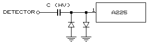
NOTE: The input protection circuit provides a limited amount of protection against transients generated in the detector and bias network. Any circuit capable of providing absolute protection would cause intolerable degradation of noise performance. For this reason, care must be exercised in the use of any preamp with high voltage detectors. Specifically, damage may result from detector breakdown, breakdown of the high voltage coupling capacitor or other component, excessively rapid rise or fall of detector bias voltage, or the addition of uncharged capacitance across the input with bias voltage applied.
In some applications, increased protection will justify an increased noise level. In this case, a resistor may be added in series with the input - normally a few hundred ohm will suffice.
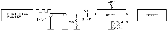
The A225 can be tested with a pulser by using a small capacitor (usually 1 to 2 pF) to inject a test charge into the input. The unit will respond to the negative-going edge of the test pulse, which should have a transition time of less than 20 ns. This negative going edge should be followed by a relatively flat part of the waveform so that it appears as a step function. For example, a square wave is a good test waveform. (Keep the square wave frequency low enough that the response to the positive-going edge can be ignored.) Alternately, a "sawtooth" waveform or a tail pulse with long fall time (> 100 µs) may be used. Charge transfer to the input is according to Q = Ct·V, where Q = total charge, Ct = value of test capacitor, and V = amplitude of voltage step. DO NOT connect the test pulser to the input directly or through a large capacitor (> 100 pF) as this can produce a large current in the input FET and cause irreversible damage.
Negative going pulse
Rise Time < 20 ns, fall time > 10 µs, or square wave.
Amplitude: 22 mV = 1 MeV (Si)
EXAMPLE: To simulate 1 MeV in silicon detector:
1 MeV (Si) = 0.044 pC
Ct = 2 pF
V = Q / Ct = 0.044 pC / 2 pF = 22 mV
i.e. a 22 mV step into 2 pF test capacitor simulates 1 MeV in silicon.
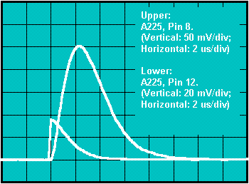
The shaping amplifier of the A225 produces a unipolar pulse at Pin 8 suitable for high resolution, high rate pulse height analysis. This output has an AC impedance of approximately 30 ohm and will drive 1 kohm loads as well as several feet of unterminated cable. In applications requiring highest linearity, load resistance should be greater than 5 kohm. This output has a quiescent D.C. output level, or Baseline, of approximately 0.8 V. In most applications the pulse should be capacitively coupled to external circuitry.
The output at PIN 12 is a timing pulse with an unloaded risetime of approximately 20 ns and a falltime of 2.8 µs capable of driving a load of 500 ohm. This output has approximately the same linearity characteristics as the shaped output at Pin 8. Grounding this pin could damage the unit.
The A225 is internally optimized for detector capacitance up to approximately 50 pF. In applications with large detector capacitance and requiring short timing pulse risetime, a compensation capacitor from 0 to 250 pF may be connected from Pin 14 to ground. The exact value should be experimentally determined with the detector connected to the input. Note that this compensation will not normally be necessary if the timing pulse is not used, or its risetime is not critical.
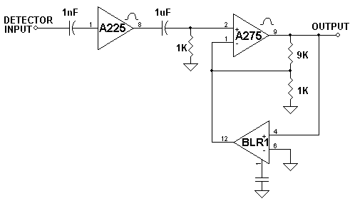
In applications requiring a bipolar pulse, the unipolar output can be differentiated with an RC differentiator. The time constant should be approximately 1.8 µs, suggested values are: C = 1 nF, R = 1.8 kohm. In most cases this pulse should be buffered in order to drive subsequent circuitry.
The A225 can be operated at high supply voltage (Vs = +25VDC) in order to maximize the dynamic range and hence minimize the overload conditions. Furthermore, pin 5 can be connected to a negative supply up to -2VDC to further decrease the overload recovery time.
Up to 100 MeV (Si) or 500 picocoulomb can be analyzed with the A225 without overloading the unit, resulting into a dynamic range of 40,000.
The X10 overload characteristics of the A225 are: < 20 µs @ Vs = +25VDC and < 40 µs @ Vs = +5VDC.
The sensitivity of the A225 can be reduced by adding the following external network:
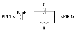
Example: C=10 pF; R=300 kOhm will reduce the sensitivity by a factor of 10. R will have to be adjusted for the individual detector load so that no overshoot occurs on the output pulse.
IMPORTANT: An equivalent detector load (typically 150-200 pF) must be present from Pin 1 to ground in order to stabalize the loop and reduce high frequency ascillation on the output pulse.
This note is intended as a guide in the use of the A225 to prevent damage due to overstress of input or output circuitry.
Input protection is described above. Please read that section carefully. The A225 input connects directly to the gate of a sensitive field effect transistor (FET). In general, any large, rapid change in voltage in the detector circuit can cause excessive input currents to flow and must be avoided. Such transients can be caused by the breakdown of the detector or the coupling or filter capacitor. Also, raising or lowering the detector bias voltage too quickly can have the same effect. The following procedures should be followed to ensure safe operation of the unit.
In order to maximize pulse drive capability, the output of the A225 is not current limited. This is not normally a matter of concern because external cpacitive coupling protects the output stage from excessive current flow in the event of a short or an attempt to drive a low impedance load, such as a terminated 50 ohm line. Such capacitive coupling normally must be used anyway between the A225 and subsequent circuitry to remove the D.C. component from the output signal. The A225 output may be damaged by shorting to ground or connection to a low impedance node of the circuit. The following guidelines should help prevent such damage.
Revised February 8, 2001