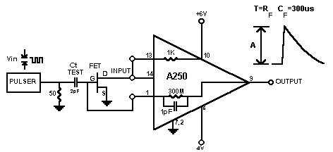
Figure 1. A250 test circuit
Figure 1. A250 test circuit
Input waveform: Square wave, or Tail pulse (Tr < 20ns, Tf > 100 µs)
Amplitude: V = Q/Ct = 500 mV per picoCoulomb for Ct = 2pF
Example: To simulate 1 MeV in Si detector: 1 MeV (Si) = 0.044 pC, 500 mV/pC x 0.044 pC = 22mV
Hence, a 22 mV step into 2pF test capacitor simulates the charge generated in a silicon detector by a particle when it loses 1 MeV of its energy.
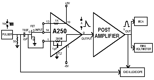
The noise of a charge sensitive preamplifier must be tested together with the post amplifier/shaper.
The A250 noise characteristics given in the specifications are associated with specific shaping time constants in the post amplifier. The post amplifier must have very low input noise as in the case of NIM electronics amplifiers or the Amptek A275, so that its contribution to the measurement is minimal. The function of the post amplifier is not only to preserve and amplify the linear information received by the charge amplifier, but also to provide a band pass filter to eliminate frequencies that contribute to noise.
Two methods are normally used to measure noise in the preamplifier: The first one is by using a Multichannel Analyzer (MCA), and the second one is with a wide-bandwidth RMS AC voltmeter.
When measuring noise of the system either by the MCA or the RMS voltmeter method the detector must be simultaneously connected with the test circuit to the input of the A250. The noise measurement in this case will include the contribution from the detector due to both its capacitance and its leakage current.
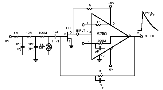
Cf < 1pF typical and Rf > 1 GOHM typical
The value of these components will effect the Fall Time of the output pulse (T = RfCf). The Rise Time of the output pulse will not be effected by the feedback components since it depends mostly on the detector capacitance, the choice of the FET and the internal characteristics of the A250. See A250 specifications.
The Gain defining component in a charge sensitive preamplifier is the feedback capacitor Cf.
Gain (Sensitivity): A = 1/Cf Volts/picoCoulomb (Cf in pF) In the case of silicon detector: A = 44/Cf in mV/MeV (Cf in pF).
Hence, for a 1pF feedback capacitor the output of the A250 will produce a 44mV pulse when
a 1 MeV particle loses all of its energy in the detector.
It is important to note that in the charge sensitive preamplifier mode of operation the
feedback resistor Rf does not effect the gain of the amplifier, it simply returns
the output of the integrating loop to the baseline.
The charge sensitive preamplifier mode of operation will give the best overall signal to noise
ratio. It is primarily used in applications where the signal from the detector is small as in
the case of solid state detectors and proportional counters.
In applications where the counting rate of the incoming pulses approaches the RfCf time constant,
the output of a charge sensitive preamplifier is shown in Figure 4.
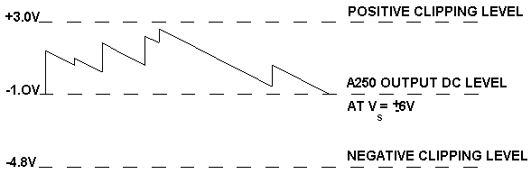
Figure 4. A250 output at high counting rates.
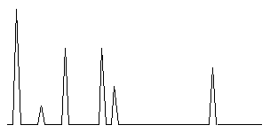
Figure 5. Post amplifier input waveform at high counting rates.
Care should be taken not to exceed the positive or negative clipping level of the A250.
The RfCf feedback components should be chosen to accommodate the expected count rates of the
particular application.
Since the charge sensitive preamplifier is AC coupled to the post amplifier/shaper with a pole
zero differentiator the resulting waveform will be as shown in Figure 5.
Cf = 2 pF and Rf = 50 kOhm
If (I) is the input current, then: Gain: Vo = (I)Rf
In this case, the Gain defining component is the Rf. The feedback capacitor Cf simply stabilizes the loop. The fall time constant will now be T = RfCf (approximately 100ns).
The topic of cooling the detector is discussed below. Nc can be minimized by using a short cable between detector and preamplifier and by minimizing any stray capacitance due to PC board layout and coaxial connectors. Typical capacitance for RG58, 50 Ohm coaxial cable is 100pF/m. The high voltage bias resistor should be chosen to have low noise, typically less than 0.5db above thermal noise with a value greater than 1 GOhm for detectors with low leakage current. The voltage applied to the detector is :
Vd = Vb - (I)R
Where: Vd is the actual voltage on the detector. Vb is the power supply voltage. (I) is the detector leakage current. R is the bias resistor.
If the leakage current in the detector is high, care should be taken to calculate the voltage drop across the bias resistor. Typically the leakage current in the detector doubles for every 8oC increase in temperature. The power supply voltage minus the voltage drop across the bias resistor should be equal to the manufacturer's recommended operating voltage for the detector at a given temperature. Also, the voltage drop across the bias resistor should not be more than 10% of the supply voltage.
The choice of the input FET is left to the user so that it can be matched to the detector and optimized to the specific application. The A250 can be used with a number of FETs whose noise performance as a function of detector capacitance and shaping time constants in the post amplifier is given in the specifications. Usually, an FET is chosen with large transconductance (gm), while matching the FET's input capacitance (Ciss), to the detector capacitance (Cd).
As the temperature decreases, the detector leakage current and noise decreases. Also, the gm of the FET increases. This results in a larger signal to noise ratio. In most FETs the gm stops increasing at approximately -140oC (1330K), because of freeze-out of the dopant of the semiconductor material. Hence, for most FETs the transconductance will be maximum at approximately 133oK and then it will drop by about 10% as the temperature reaches 77oK (Liquid Nitrogen, LN2). In many experiments requiring cooling, the detector is placed at the LN2 temperature, and the FET is placed further away or heated, so that its temperature is near 133oK. Example of FETs used in experiments requiring cooling are: 2N4416, 2N6451, 2SK152, 2N6550, and 2N3823.
In cryogenic experiments where both the detector and the FET must be at Liquid Helium temperature (4oK), different FETs must be used. The manufacturing process of these FETs allows them to be cooled down to 4oK. An example is the SONY GaAs MESFET SGM2006M (previously known as 3SK164). Use of this FET, however, at higher temperatures (near 133oK) is not recommended because its noise performance will be inferior to the FETs previously mentioned.
Most low noise FETs exhibit a noise of about 100 - 120 electrons RMS at room temperature. This noise decreases to approximately 15 - 25 electrons RMS as the temperature reaches 133oK.
In applications where the detector, input FET and feedback components are located further away unterminated coaxial cables may be used to make the electrical connections. The maximum length of these cables is dependent on FET characteristics, and detector, feedback and load capacitance, but usually at least 2m is possible. Two coaxial cables will be needed, one to connect the output of the A250 to the feedback network in the cryostat, and other to connect the A250 input to the FET Drain. Since the addition of the cable will decrease the closed loop phase margin of the preamplifier, the A250 should be configured with this in mind. The feedback capacitor should be as small as possible, consistent with the gain, linearity, and risetime requirements. If necessary, a compensation capacitor from Pin 6 to ground can be added to lower the frequency of the dominant pole of the A250.
Probably the most important consideration with a remote FET is proper grounding and shielding. The outer conductor of the Drain (A250 input) cable should be connected to ground at the A250 end, and to the FET Source at the other end.
For the feedback cable, the outer conductor should be connected to ground at the A250 end, and left unconnected at the other end.
The High Voltage bias to the detector should be decoupled with a capacitor to the FET Source node in the cryostat. Any additional shielding around the detector and FET should be connected to this node. An additional low impedance ground cable from this node back to the A250 may also be helpful.
DCVout = -1V - Rf * (gate leakage current)
For an FET with gate leakage current < 50 pA. DCVout must not be allowed to reach the clipping level. If DCVout is to be about -2V, then Rf must be <20 GOhms.
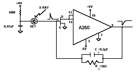
Figure 6. DC Coupled PIN-Photodiode to the A250
For DC coupled detector systems, the detector leakage current must be added to the gate leakage current in the DCVout formula above. Usually, detector leakage dominates FET leakage. For example, with a 1nA detector leakage current and DCVout= -2V, Rf must be less than 1GOhm.
In very high resolution systems measuring X-Rays or Gamma Rays other methods are used in order to discharge the feedback capacitor. These methods are optical pulsed feedback, and transistor reset circuits. (see ref. 5,6)
The shaping time constant in the post amplifier should be selected for each application. For room temperature experiments the shaping time constant is usually between 0.5 µs and 3 µs. For cooled experiments greater than 3 µs is used.
There are many types of shaping methods used to filter out low and high frequency noise (RC-RC, Gaussian, Cusp, Triangular, Trapezoidal and others). The most commonly used is the Gaussian shaper. An example of a 3 pole Gaussian shaper is given at the back of the A250 specifications and of a 5 pole Gaussian shaper at the back of the A275 specifications. Increasing the number of poles normally improves the symmetry of the output pulse, which improves the noise and count rate performance of the system.
Example: For a cooled system to reach a total noise of about 20 electrons RMS (180 eV FWHM, Si):
The A250 did not enter into the considerations because its noise contribution is negligible compared to that of the input FET and detector.
A250 Application Notes also available in PDF format.
Revised February 8, 2001