
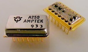
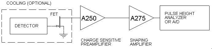
The A250 is a hybrid state-of-the-art Charge Sensitive Preamplifier for use with a wide range of detectors having capacitance from less than one, to several thousand picofarads. Such detectors include silicon, CdTe, CZT, and HgI2 solid state detectors, proportional counters, photomultiplier tubes, piezoelectric devices, photodiodes, CCD's, and others.
To permit optimization for a wide range of applications, the input field effect transistor is external to the package and user selectable. This feature is essential in applications where detector and FET must be cooled to reduce noise. In all applications, it allows the FET to be matched to the particular detector capacitance, as well as to noise and shaping requirements. In larger quantities, the A250 may be specially ordered with an internal FET.
The noise performance of the A250 is such that its contribution to FET and detector noise is negligible in all charge amplifier applications, i.e., it is essentially an ideal amplifier in this respect.
The internal feedback components configure the A250 as a charge amplifier; however, it may be used as a high performance current or voltage preamplifier by choice of suitable feedback components.
While these preamps were designed for multidetector satellite instrumentation, their unique characteristics make them equally useful in a broad range of laboratory and commercial applications.
Features
|
Applications
|
Sensitivity can be reduced by connecting Pin 2 and/or 3 to Pin 1, thus providing Cf = 3, 5, or 7 pF. Additional external capacitors can be ad for further reduction of gain. In general, the sensitivity is given by A = 1/Cf (pF) V/pC. For silicon, the sensitivity is A = 44/Cf (pF) mV/MeV.
Data presented in Figure 1 is representative of results obtained with recommended FETs, and is characteristic of the FET and shaping time constants, rather than the A250, which is effectively noiseless. In general, the choice of input FET is based on its noise voltage specification (nV/root Hz) and its input capacitance (Ciss).
For low capacitance detectors, a FET with small Ciss should be chosen, such as 2N4416 or 2SK152.
For very high capacitance detectors, two or more matched high Ciss FETs such as the 2N6550 may be paralleled to achieve the best noise performance.
| Polarity | Inverse of input |
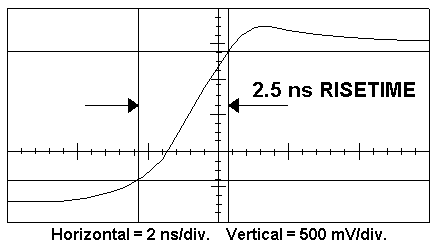
| Rise Time | 2.5 ns at 0 pF input load with 2SK152 4.5 ns at 100 pF input load with 2N6650 or 2SK152 Figure 2, Figure 3. |
| Output Impedance | 100 ohm |
| Integral Nonlinearity | < 0.03% for 0 to +2 V unloaded < 0.006% for 0 to -2 V unloaded |
| Decay Time Constant | 300 Mohm x Cf = 300 µs, 900 µs, 1.5 ms, 2.1 ms User selectable T=Rf Cf |
| Positive Clipping Level | > +2.8 V |
| Negative Clipping Level | < -4.6 V |
| Gain-Bandwidth Product | fT > 300 MHz with 2N4416 FET, Figure 4. fT > 1.5 GHz with two 2SK147 FETs, Figure 4. |
| Operating Voltage | ±6 V, (±8 V maximum) |
| Operating Current | ±1.2 mA plus the FET drain current (Ids). Where: Ids (mA) = 3/R (kohm) - 0.25. As a special case, the internal 1 K resistor may be used for R, by connecting Pin 13 to 14, giving Ids = 2.75 mA. |
| Power Dissipation | 14 mW + 6[Ids] |
| Variation of Sensitivity with Supply Voltage | < 0.15%/V at ±6 V. |
| Temperature Stability | < 0.1% from 0 to +100 ºC < 0.5% from -55 to +125 ºC |
| Operating Temperature | -55 to +125 ºC |
| Storage Temperature | -65 to +150 ºC |
| Screening | Amptek High Reliability |
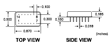
| Package | 14 pin hybrid DIP (metal) |
| Warranty | One year |
| Test Board | PC-250 |
| Options | - Internal FET (consult factory) - NASA GSFC S-311-P-698 screening - Amptek High Reliability Screening |
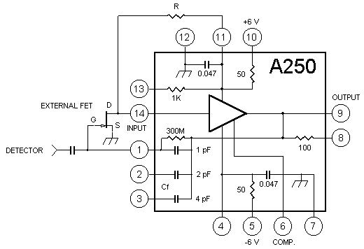
| Pin 1 | 300 Mohm resistor in parallel with 1 pF feedback capacitor. Connect this pin to the detector and the gate of the FET |
| Pin 2 | 2 pF feedback tap. |
| Pin 3 | 4 pF feedback tap. |
| Pin 4 | -6 V direct. |
| Pin 5 | -6 V through 50 ohm. |
| Pin 6 | Compensation (0-30 pF to ground) for low closed loop gain configuration (where a large feedback capacitor is used together with small detector capacitance). |
| Pin 7 | Ground and case. |
| Pin 8 | Output through 100 ohm. |
| Pin 9 | Output direct. |
| Pin 10 | +6 V through 50 ohm. |
| Pin 11 | +6 V direct. |
| Pin 12 | Ground and case. |
| Pin 13 | Provide 2.75 mA drain current to the external FET by connecting pin 13 to 14. (See operating current specifications.) |
| Pin 14 | Input. Should be connected to the drain of the FET. This pin is held internally at + 3 Volts. |
as a function of detector capacitance, input FET, feedback capacitor, and shaping times
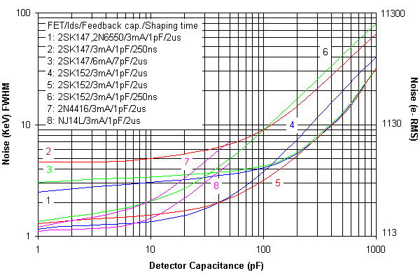
Figure 1.
versus detector capacitance and FET
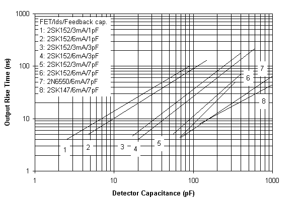
Figure 2.
Configured as a charge sensitive preamplifier
2SK152/3mA, Rf = 300 Mohm, Cf = 1 pF, Cd = 0 pF
Configured as a Transimpedance Amplifier (current to voltage)
2N4413/3mA, Rf = 60 kohm, Cf = 0 pF, Cd = 0 pF
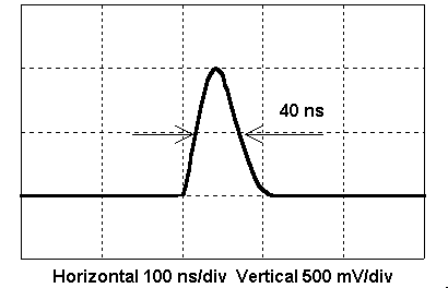
Figure 3.
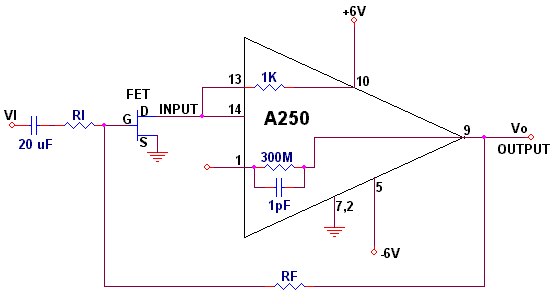
Typical RF = 1M, RI = 10K
GAIN: Vo = VI(RF/RI)
for low capacitance FET: 2N4416 (Ciss = 4 pF, Ids = 3 mA)
for high capacitance FET: 2 x 2SK147 (Ciss = 180 pF, Ids = 1.5
mA each)
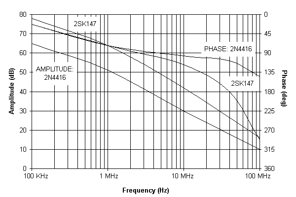
Figure 4.
There is additional information available in the A250 application note (AN250-2 Rev. 3)..
Revised February 8, 2001