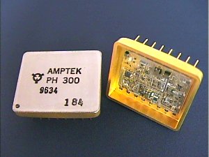
Model PH300 is a high performance, thin film hybrid, peak-hold unit, designed to track and hold the peak of analog input signals with rise times (10% to 90% of Vmax) as short as 250 ns. The unit also has the lowest Droop Rate of the held voltage available and consumes less than 36 mW of power in quiescent mode. While this unit was designed for use in satellite instrumentation, the following unique characteristics make it equally useful in a broad range of space, laboratory and commercial applications.
Features
|
Applications
|
Principle of Operation and Functional Diagram
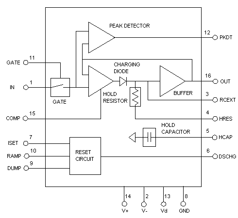
The PH300 is a peak-hold device, designed to track an analog input pulse and keep the maximum amplitude as a peak voltage on a hold capacitor. Major functional elements are identified in the functional diagram above. An innovative boot-strap circuit in the input stage of the output buffer amplifier, minimizes the droop error which occurs during periods of long peak-hold duration. Inputs to the IN terminal are gated through a linear gate (gate input), which is controlled by a TTL compatible logic signal. When the gate is open (gate high), the input signal is sensed by the error amplifier. When the gate is closed (gate low), the input to the error amplifier is grounded and the input signal does not have any effect on the output of PH300.
During the rise time of the input signal, the hold capacitor is charged through a charging diode and a hold resistor. For the PH300, this mode of operation is referred to as the charging mode. The device goes into hold mode as soon as the input reaches Vmax and starts to decay. This state can be terminated by discharging the hold capacitor. When the circuitry to accomplish this is enabled, the PH300 is placed in discharge mode. A special case of the discharge mode is the tracking mode. Additional information on each of these operational modes follows.
Charging mode
The hold capacitor is charged during the rise time of the input signal. The rise time of the input pulses can be as short as 250 ns. When the PH300 is in charging mode, negative feedback is applied to the amplifier through the high impedance output buffer. Under this condition, the output voltage follows the input signal and the peak detector logic output is in the inactive state. The feedback circuit brakes immediately after the input goes through a maximum level and starts decaying. The PH300 then enters hold mode.
Hold mode
In this mode, the charging diode is reverse biased and the voltage across the hold capacitor is held equal to Vmax. The peak-detector logic output is in the active state. The leakage currents of the components connected to the hold capacitor causes it to discharge. The rate of this discharge is the droop rate of the PH300.
Discharge mode
The hold capacitor could be intentionally discharged by enabling the reset circuit within the PH300. Two types of reset are possible. They are: (i) ramp or linear reset and (ii) dump or fast reset.
In ramp discharge mode, the hold capacitor is discharged through a constant current draw, which is set with an external resistor or by an external current source. Constant current discharge results in a linear decrease of the held voltage. This operating mode is used in Wilkinson type analog to digital converters.
In fast discharge mode, the hold capacitor is discharged through a large current draw for a short period of time. The frequency and duration of this mode of operation determines the upper limit of power consumption for the device.
Tracking mode
Negative feedback to the amplifier could become active (and correspondingly the peak-detector logic output goes to the inactive state) in discharge mode operation, if the hold capacitor voltage becomes less than or equal to the voltage at the amplifier input. Therefore, if the discharge rate of the hold capacitor is higher than the decay rate of the input signal, the output of the PH300 will follow the input even when the signal is decaying. This mode of PH300 operation is referred to as the tracking mode.
Specifications
| Input Characteristics | |
|---|---|
| SIGNAL - Analog | Range: 0 to (V - 1.5V) Input impedance: > 1 kohm Rise time (10% - 90%): 250 ns (min) |
| LINEAR GATE CONTROL - Digital | Logic level: TTL Gate open: HIGH Gate closed: LOW Gate turn on/off: 40 ns (60 ns max) |
| RESET CONTROL - Digital | Ramp slew rate: 5 V/µs to 0.001 V/µs Ramp control: TTL Ramp active: LOW Fast reset: < 800 ns (dump mode) Dump control: TTL Dump active: LOW |
| Output characteristics | |
|---|---|
| ANALOG | Range-load: >5 kohm 0 to (V - 1.5V) (typical) Output slew rate: 30 V/µs Droop rate: < 1 µV/µs (-55 ºC to +85 ºC) < 10 µV/µs (+85 ºC to +125 ºC < 10 nV/µs (1 nV/µs typ) @ +25 ºC Linearity: ± 0.01% (typical) DC offset: ± 2 mV (max) |
| DIGITAL PEAK DETECT | Logic level: TTL V: > V HIGH V: < V LOW Propagation delay: < 500 ns (typical) |
| HOLD CAPACITOR | Internal: 470 pF ±5% >External: 50 pF - 1000 pF (optional) |
| Environment | |
|---|---|
| CASE TEMPERATURE | Operating: -55 ºC to +125 ºC Storage: -55 ºC to +150 ºC |
| RADIATION | Hardness: 10 rad(Si) (optional with PH300RH only) |
| SCREENING | Amptek High Reliability |
| POWER SUPPLY | Quiescent power: <36 mW @ -5V/+10V |
| ANALOG | V: +5 V to +12 V V: -5 V to -6 V Quiescent I: < 2.4 mA (-55 ºC to +125 ºC) Quiescent I: < 2.4 mA (-55 ºC to +125 ºC) |
| DIGITAL | V: +5 V Quiescent I: < 0.01 mA (-55 ºC to +125 ºC) |
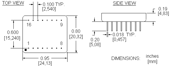
| PACKAGE | Hermetic, 16 pin hybrid, 600 mil DIP |
Pin Description
| 1 | IN is the analog input of the PH300. This input accepts a positive signal. The input signal should not be driven greater than the positive analog power supply, or less than -0.5 V. Schottky diode input protection is recommended. Range is 0 to (V - 1.5V). |
| 2 | V (-5 V to -6 V) |
| 3 | RCEXT is a node that allows connection of an external hold resistor and hold capacitor. When internal hold components are used, RCEXT is left unconnected. |
| 4 | HRES is the node of the internal hold resistor. |
| 5 | HCAP is the node of the internal hold capacitor. This node is normally connected to HRES and DSCHG. | 6 | DSCHG is a node of the current generator used to reset the hold capacitor of the PH300. The RAMP reset current is set by an external current source or an external resistor. This node is in a high impedance state when PH300 is in hold mode. Normally this node is connected to the HCAP node. |
| 7 | ISET is a node of the current mirror that sets the discharge
current. This node sinks positive current. The discharge current is twice
the current at this node. An external resistor R can be connected between
ISET and ground. In this case the reset current is approximately set to
2*(V + 0.6V)/(R + 500 ohm).
NOTE! To ensure proper PH300 tracking mode operation, a reset current must be set regardless of the reset scheme (RAMP or DUMP) used to discharge the hold capacitor. |
| 8 | GND |
| 9 | DUMP (active low) is a TTL compatible signal used for fast reset of the PH300. This signal must be used only in conjunction with the RAMP signal. The DUMP signal can be active only when RAMP is active. A LOW state of this signal causes the discharge current to peak up to 20 mA, causing fast discharge of the hold capacitor. The duration of the DUMP signal should be keep as short as possible, since the high reset current increases substantially the power consumption of the PH300. A fixed duration of 1 µs usually is sufficient to completely reset the built in hold capacitor. The PKDT signal can be used as an indicator for the discharge of the hold capacitor and may provide a function to control the duration of the DUMP signal. |
| 10 | RAMP (active low) is a TTL compatible input that controls the linear discharge of the PH300. When this signal is LOW, the DSCHG node sinks current that resets the hold capacitor. Since the reset current is constant, the output of PH300 decays linearly. | 11 | GATE (open high) is a TTL compatible logic input that controls the linear gate of the PH300. When GATE is in an active HIGH state, the linear gate is open and the error amplifier of the PH300 can sense the input signal. When GATE is inactive, the error amplifier input is tied to ground. |
| 12 | PKDT is an TTL output that indicates the state of the PH300. When this signal is LOW, the PH300 is in a hold mode. |
| 13 | V (+5 V) |
| 14 | V (+5 V to +12 V) |
| 15 | COMP is a node for frequency compensation of the PH300 when an external hold capacitor is used. In this case a resistor between 20 and 100 ohms can be used to reduce output signal oscillations. This resistor must be connected between COMP and V. When the internal hold capacitor is used, COMP must be connected to V. |
| 16 | OUT is the analog output of the PH300. This output is protected for short circuits to ground or any voltage between ground and the positive analog power supply. WARNING! Shorting this output to any negative voltage may destroy the PH300 circuit. This output can drive capacitive loads up to 50 pf (typical). For higher capacitive loads, use a resistor of 50 to 100 ohms in series with OUT. Range is 0 to (V - 1.5V), typical. |
Application notes
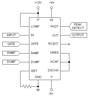
Figure 1. - PH300 typical wiring diagram.
Figure 1 shows a typical wiring diagram of PH300 using the internal hold and reset components. The board design should prevent any possible paths for leakage currents to the DSCHG, HCAP, HRES and RCEXT nodes.
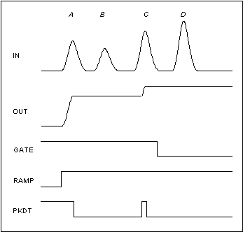
Figure 2. - Gate function of PH300.
Figure 2 shows the use of the linear gate. Four pulses marked A, B, C, and D are applied to the input of PH300. The linear gate is open for the first three pulses and closed for the last pulse, D. The PH300 is not discharged between the pulses. Only the peaks of the pulses A and C will be detected. Pulse B passes through the linear gate. However, since its amplitude is less than the held amplitude of pulse A, there is no change of the PH300 output. Pulse D does not affect the held peak voltage of pulse C because the linear gate is closed.
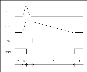
Figure 3. - Timing diagram illustrating RAMP reset of PH300.
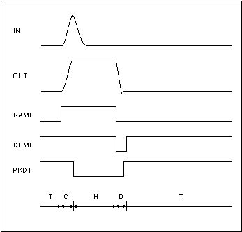
Figure 4. - Timing diagram illustrating DUMP reset of PH300.
Figures 3 and 4 illustrate the modes of operation of the PH300 with RAMP and DUMP reset of the hold capacitor. The linear gate is open. The modes of operation are indicated with bold characters as follows:
C = charging mode
D = discharge mode
H = hold mode
T = tracking mode
PH300 Specifications in PDF format (67 kB)
Hybrid Selection Guide | Home Page | Products | Price list | Company Profile | Press Release
Revised February 8, 2001

