Model A203 is a Charge Sensitive Preamplifier/Shaping Amplifier developed especially for instrumentation employing solid state detectors, proportional counters, photomultipliers or any charge producing detectors in the pulse height analysis or pulse counting mode of operation.
While this unit was specifically designed for satellite instrumentation, the following unique characteristics make them equally useful for space, laboratory and commercial applications:
| For positive unipolar output (Pin 8) |
210 mV/MeV (Si); 262 mV/MeV (Ge); 4.8 x 10 V/coulomb; 0.76 µV/electron |
| For bipolar output (Pin 9) |
115 mV/MeV (Si); 144 mV/MeV (Ge); 2.6 x 10 V/coulomb; 0.42 µV/electron. |
| Unipolar |
8 KeV FWHM (Si); 6.4 KeV FWHM(Ge); 1.4 x 10 coulomb rms; 875 electrons rms |
| Bipolar |
12 KeV FWHM (Si); 10 KeV FWHM (Ge); 2.2 x 10 coulomb rms |
| Noise Slope (typical) | 100 eV/pF (Si); 80 eV/pF (Ge); 1.81 x 10 coulombs/pF |
| Dynaimic Input Capacitance | 3,500 pF |
| Polarity | Negative |
| Protection | Back-to-back diodes to ground |
| Rise time | 50 ns |
| Fall time | 30 µs |
| AC Output impedance | 50 ohm |
| Time constants | 250 ns |
| Positive Unipolar, Pin 8 | AC output impedance: 85 ohm Dynamic range: 75% of Vs Pole-zero cancellation: External 1 Mohm between Pin 12 and 13 |
| Bipolar, Pin 9 | AC output impedance: 2 kohm Dynamic range: 35% of Vs |
| Operating Voltage | +10 to +18 VDC |
| Operating Current | 1.4 mA quiescent @ 15V |
| Temperature | -55º to +70º C operational |
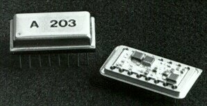
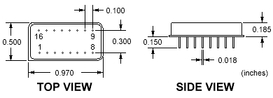
| Package | 16 Pin Dual In-Line (Metal) |
| Screening | Amptek High Reliability |
| Warranty | One year |
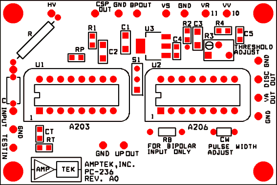
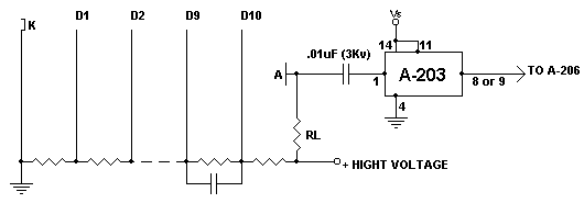
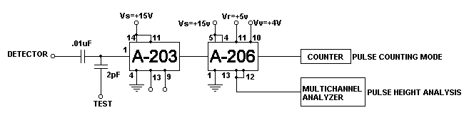
The PC-236 is a printed circuit board designed to facilitate testing of the A203/A206 system. It provides the test circuit for the charge sensitive preamplifier, as well as the voltage references for the discriminator. All components are laid out on a ground plane in order to minimize noise and external pickup.
The A203 has two parts:
1) A Charge Sensitive Preamplifier (CSP)
2) A Shaping Amplifier (SA).
The output of the CSP is internally connected to the input of the SA.
Power to the CSP and SA are provided separately in order to provide maximum flexibility for independent operation. However, for normal operation Pin 11 and Pin 14 should be connected to Vs. Supply is internally bypassed. Care should be taken in circuit layout and in some applications power supply decoupling may be helpful. If the leads of the A203 are left long or the unit is socketed, the unconnected Pins 2, 3, 6, 7, 10, 15, 16 should be grounded in order to minimize pick-up.
The sensitivity of the CSP is defined by: G = 44/C in mV/MeV (Si), where C is the feedback capacitor (in pF). The feedback capacitor in the A203 is 2 pF. If a lower sensitivity is desired, an external capacitor may be added between Pins 1 and 13. A capacitor with good temperature stability should be used and the leads should be kept short.
The detector must be capacitively coupled to Pin 1 with a capacitor of adequate voltage rating.
If the output of the CSP (Pin 13) is to be connected to external circuitry it must be coupled with an external capacitor. This output can drive several feet of unterminated coaxial cable.
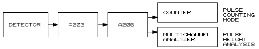
The SA has two outputs: 1) Unipolar (Pin 8) which is single integration - single differentiation. 2) Bipolar (Pin 9) which is single integration - double differentiation. Either output can drive the A206, which has an input coupling capacitor. If the unipolar output (Pin 8) is to be connected to other external circuitry it MUST be capacitively coupled.
If pole-zero cancellation is required at the unipolar output in order to minimize the baseline shift, a 1 Mohm resistor must be externally added between Pins 12 and 13.
The A203 can be tested with a pulser by using a small capacitor to inject a negative test charge into the input. The unit will respond to the negative-going edge of either a square wave or a tail pulse with long fall time (> 10 µs). In either case the negative-going transition should be less than 20 ns. Charge transfer in the circuit is according to Q = C·V, where Q = total amount of charge delivered to input, C = test capacitor and V = amplitude of the pulse. Use only a small capacitor in this circuit (1 to 10 pF). DO NOT connect a low impedance pulser through a large capacitor when testing as this will overdrive the input and may damage the unit. Example: A 22 mV tail pulse across a 2 pF test capacitor is equivalent to 1 MeV energy loss in silicon (3.5 eV/pair) and will produce a 210 mV unipolar pulse at Pin 8.
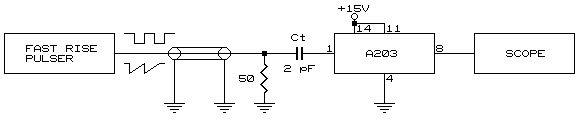
EXAMPLE: To simulate 1 MeV in silicon detector:
1 MeV (Si) = 0.044 pC
Ct = 2 pF
V = Q / Ct = 0.044 pC / 2 pF = 22 mV
i.e. a 22 mV step into 2 pF test capacitor simulates 1 MeV in silicon.
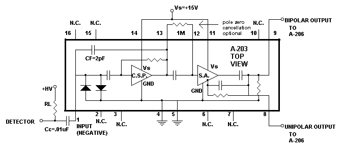
| Pin 1 | Charge Sensitive Preamplifier Input |
| Pin 2 | No connection |
| Pin 3 | No connection |
| Pin 4 | Ground and case |
| Pin 5 | Ground and case |
| Pin 6 | No connection |
| Pin 7 | No connection |
| Pin 8 | Unipolar shaping Amplifier Output |
| Pin 9 | Bipolar Shaping Amplifier Output |
| Pin 10 | No connection |
| Pin 11 | Vs Shaping Amplifier (+10 V to +18 V) |
| Pin 12 | Shaping Amplifier Input |
| Pin 13 | Charge Sensitive Preamplifier Output |
| Pin 14 | Vs C.S. Preamplifier (+10 V to +18 V) |
| Pin 15 | No connection |
| Pin 16 | No connection |
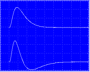
 Horizontal Scale: 10µs/div Vertical Scale: 10mV/div Top Trace: Input to test capacitor -22mV = 1 MeV(Si) Bottom Trace: Output of CSP (A-203, Pin 13) |
 Horizontal Scale: 500ns/div Top Trace: Unipolar output of SA (A203, Pin 8) Vertical Scale: 50mV/div Bottom Trace: Bipolar output of SA (A203, Pin 9) Vertical Scale: 100mV |
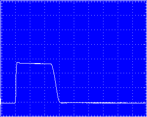 Horizontal Scale: 5V Vertical Scale: 2µs LLD Output-Positive (A206, Pin 9) | |
Revised February 8, 2001