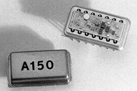

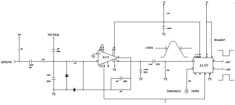
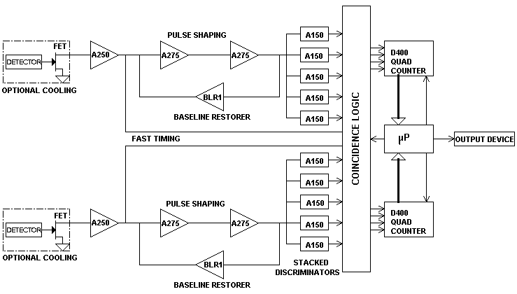
The A150 is a high performance hybrid pulse amplitude discriminator developed for use in precision pulse spectroscopy.
Its low power dissipation (17mW), high speed (>4 MHz), and radiation hardness (106 Rads), make it ideal for space flight use. The A150 is packaged in a standard 14-pin hybrid DIP.
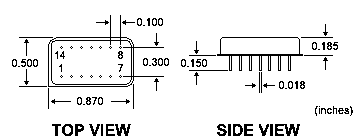
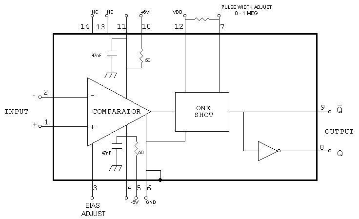
| PIN | FUNCTION |
| 1 | Non-Inverting Input |
| 2 | Inverting Input |
| 3 | Bias Adjust (resistance to PIN 4 reduces operating current) |
| 4 | -Vs Direct | 5 | -Vs through 50 ohms |
| 6 | Case and Ground |
| 7 | Pulse Width Adjust (must be connected to PIN 12 either directly for minimum pulse width, or through a resistor) |
| 8 | Output (positive) | 9 | Output (negative) |
| 10 | +Vs through 50 ohms |
| 11 | +Vs Direct |
| 12 | VDD bias for output CMOS one-shot |
| 13 | N.C. |
| 14 | N.C. |
| Absolute Maximum Ratings | |
| Supply Voltage Vs | +,- 8V |
| CMOS Supply VDD | + 18V |
| Input Voltage | +,- Vs |
| Operating Temperature Range | -55oC to +110oC |
| Storage Temperature Range | -65oC to +110oC |
| Lead Temperature Range (Soldering, 10 sec.) | 300oC |
| ELECTRICAL CHARACTERISTICS | |||||
| PARAMETER | SYMBOL | MIN | TYP | MAX | UNITS |
| Output Pulse Width-Positive | TWP | 160 | 195 | 210 | ns |
| Output Pulse Width-Negative | TWN | 150 | 185 | 200 | ns |
| Output Pulse Delay-Positive | TDP | - | 70 | 120 | ns |
| Output Pulse Delay-Negative | TDN | - | 60 | 80 | ns |
| Input Threshold Offset | VOS | - | +,-1 | +,-5 | mV |
| Supply Voltage | VS | +,-4.5 | +,-6 | +,-8 | V |
| Supply Current | IS | +,-1.3 | +,-1.5 | +,-1.7 | mA |
| CMOS Supply | VDD | +4 | +10 | +18 | V |
| Power Consumption | PD | - | 17 | - | mW |
| Input Offset Drift | TCVos | - | -30 | +,-10 | uV/oC |
| Minimum Pulse Detected | VTmin | - | 15 | - | mV |
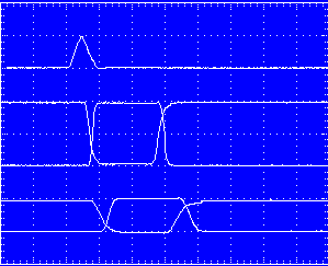 Horizontal Scale: 100ns/div Vertical Scale: 5V/div Upper Trace: Input Pulse Middle Trace: Outputs at VDD= +10V Lower Trace: Outputs at VDD= +5V |
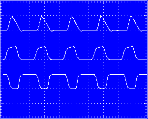 Horizontal Scale: 100ns/div Vertical Scale: 10V/div Upper Trace: Input Pulse at 5 MHz Middle Trace: Pin 9 Output at VDD= +10V Lower Trace: Pin 8 Output at VDD= +10V |
Revised February 8, 2001