![[a111 19k]](a111.jpg)
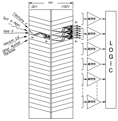
Designed for direct applications in the field of aerospace and portable instrumentation, mass spectrometers, particle detection, imaging, laboratory and research experiments, medical electronics and electro-optical systems.

Designed for direct applications in the field of aerospace and
portable instrumentation, mass spectrometers, particle detection,
imaging, laboratory and research experiments, medical electronics
and electro-optical systems.
Model A111 is a hybrid charge sensitive preamplifier, discriminator, and pulse shaper developed especially for instrumentation employing microchannel plates (MCP), channel electron multipliers (CEM), photomultipliers, proportional counters and other low capacitance charge producing detectors in the pulse counting mode. While this unit was developed for NASA's deep space probes, the following unique characteristics make it equally useful for space, laboratory and commercial applications:
| Vs = +5 V, T = +25 °C | |
|---|---|
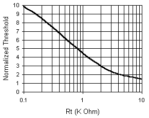
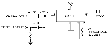
| Threshold | Model A111 has a nominal threshold referred to the input of 8 x 10 coulomb. This is equivalent to 5 x 10 electrons. The threshold can be increased by the addition of a resistor between Pin 7 and 8. Shorting these pins together produces the maximum increase (approximately 10x). See Figure 1. |
| Stability | +5%, -2% of +25 ºC threshold, 0 to +50 ºC. |
| Threshold supply voltage coefficient | -0.8%/V typical. |
| Noise (typical) | 4.4 x 10 coulombs RMS; 5.5% of nominal threshold. |
| Detector capacitance | 0 to 250 pF. |
| Protection | 300 ohm resistor in series with input followed by back-to-back diodes to ground. |
| Risetime | 25 ns. |
| Falltime | 220 ns with CLOAD = 5 pF; 90 ns with CLOAD = 5 pF and RLOAD = 2 kohm. |
| Width | 260 ns at threshold, 310 ns at 10x threshold, with CLOAD = 5 pF. |
| Amplitude | 4.7 volts (approximately 95% of Vs.) |
| Protection | Diodes to ground and Vs. |
| Cout rate | 2.5 x 10 CPS periodic. |
| Pulse pair resolution | 1) Normal: 350 ns; two identical 10x threshold pulses. 2) Overload: 800 ns; 100x threshold followed by 10x threshold. |
| Operating voltage | +4 to +10 VDC. |
| Operating current (typical) | 1.3 mA quiescent. 1.4 mA @ 10 CPS. 1.9 mA @ 10 CPS Operating current is essentially independent of Vs. |
| Temperature | -55 to +85 ºC operational. |
| Screening | Amptek High Reliability (Optional NASA GS/FC S-311-P-698) |
| Warranty | One year. |
| Radiation resistance | > 100k rad(Si) |
| Weight | 2.6 g |
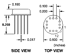
| Package | 12-pin TO-8 case. (6-pin SIP available as model A111F) |
| Accessories | PC-21 test board. |
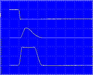
| Horizontal scale: | 200 ns/div. |
| Top trace: | Input test pulse through 2 pF capacitor. The A111 responds during the risetime of the test pulse. Vertical scale: 100 mV/div. |
| Middle trace: | Analog pulse, Pin 7 Vertical scale: 0.5 V/div. |
| Bottom trace: | Discriminator output, Pin 5, driving a 1 kohm load at Vs = +5V Vertical scale: 2 V/div. |
Due to the high sensitivity of the A111, care should be taken in circuit layout. In general, ground plane construction is recommended, with all ground pins (1,3,4,6,10,11, and 9) connected to this plane. Input and output lines should be kept well separated and in most cases shielding will be necessary. Particular attention should be paid to the detector ground connection to avoid multiple pulsing and oscillation due to feedback. The supply voltage is internally decoupled which prevents the A111 from responding to supply line transients of up to 100 mV amplitude. While this is normally adequate, in some applications external bypassing (typically 10 nF) may be helpful. The PC-21 may be used as an example of appropriate layout techniques.
While specifications are given for operation at +5 V, the characteristics of the A111 are relatively unaffected by changes in supply voltage from 4 to 10V. Parameters critical to a particular application should be checked at the actual operating voltage.
The A111 has an internal input protection network, including a coupling capacitor, as shown:
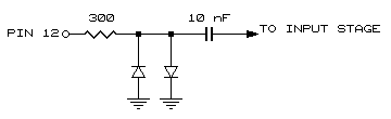
The detector anode should normally be capacitively coupled to Pin 12 with a capacitor of adequate voltage rating. In some applications, where the detector cathode is operated at negative potential, the anode can be directly connected to Pin 12.
The A111 will respond to a negative pulse of 8 x 10 coulombs or greater. The threshold may be increased by the connection of a resistor between Pins 7 and 8. Approximate values are given in Figure 1.
While this device is optimized for negative input pulses, it will respond to positive input pulses greater than approximately 2x the negative threshold. Because the specifications provided herein apply to negative input, the user should measure all relevant operating characteristics for any positive-input applications.
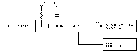
The A111 can be tested with a pulser by using a small capacitor (usually 1 or 2 pF) to inject a test charge into the input. The unit will trigger on the negative-going edge of the test pulse, which should have a transition time of less than 20 ns. This negative going edge should be followed by a relatively flat part of the waveform so that it appears as a step function. For example, a square wave is a good test waveform. (When using a square wave, it should be noted that the unit will respond to the positive-going edge also, at amplitudes above 2x threshold). Alternately, a "sawtooth" waveform or a tail pulse with long fall time (> 1 µs) may be used.
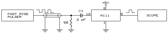
Trise: < 20 ns (negative-going edge)
Amplitude: 500 mV/picocoulomb; 4 mV at the nominal threshold.
Charge transfer to the input is according to Q = Ct·V, where Q = total charge, Ct = value of test capacitor, and V = amplitude of voltage step. DO NOT connect the test pulser to the input directly or through a large capacitor (> 100 pF) as this can produce a large current in the input transistor and cause irreversible damage.
The output circuit of the A111 is a PNP transistor with a 6 kohm collector load to ground:
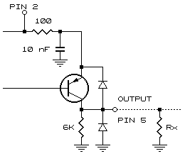
This circuit directly drives CMOS inputs with wide voltage swing and thus excellent noise immunity. The high value (6 kohm) load resistor minimizes both internal ground currents and power consumption in critical applications. In applications where load capacitance is significant and high count rate performance is important, the addition of an external resistor Rx from Pin 5 to ground will shorten the fall time of the output pulse. A typical value for load capacitance of 10 to 50 pF, is 2 kohm. At the expense of pulse amplitude, low impedance circuits may be driven, e.g. terminated coaxial cable. For example, terminated 50 ohm cable can be driven with a pulse amplitude of 1.4 V (Vs = 5 V).
To interface the A111 directly with TTL, a value for Rx must be chosen to sink the required low level input current of the TTL device. for example, for low power devices requiring Iin = 0.4 mA at 0.4 V, the maximum value for Rx in parallel with the 6 kohm is 1 kohm. For devices requiring more than 2 mA current sinking, an inverting NPN transistor interface between the A111 and the input is recommended.
Due to its hermetic seal and small size, the A111 is well suited to use within a vacuum chamber. In such applications care should be taken to avoid electrical discharge near the input which can damage the unit and VOID WARRANTY.
Use care in soldering leads - avoid overheating.| Pin 1 | Ground and Case |
| Pin 2 | Vs (+4 to +10 VDC) |
| Pin 3 | Ground and Case |
| Pin 4 | Ground and Case |
| Pin 5 | Output |
| Pin 6 | Ground and Case |
| Pin 7 | Analog monitor |
| Pin 7,8 | Threshold adjustment |
| Pin 9 | No connection |
| Pin 10 | Ground and Case |
| Pin 11 | Ground and Case |
| Pin 12 | Input |
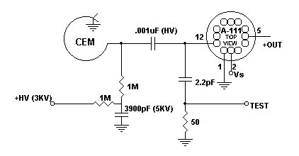
The PC-21 is a printed circuit board designed to facilitate testing of the A-111 or A-111F. In addition to testing circuitry, it provides component locations for use with detectors. Ground plane construction minimizes external pick-up.
![[pc-21 layout]](pc21b.gif)
| INPUTS | |
| IN | Detector input; Pin 12, Pin 1 for A111F (should be AC coupled with a high voltage capcitor). |
| DET | Provides post to connect the detector and input capacitor |
| TEST IN | Input to test circuit as described in specifications |
| Vs | Pin 2 (Pin 5 A111F); Supply voltage (+4 to +18 VDC). |
| HV | Provides post to connect the detector to the high voltage supply through a resistor. |
| OUTPUTS | |
| OUT | Pin 5 (Pin 6 A111F) |
| A OUT | Pin 7 (Pin 4 A111F) |
| COMPONENTS | |
| C1, C2, C3 | Filter capacitors (1uf, 4.7uf, 0.1uf) |
| Ct | Test capacitor (2 pF) |
| Ro | Test pulse termination resistor (50 ohm) |
| Rx | External load resistor (see specifications) |
| Rt | Threshold adjust resistor |
| R | Detector bias resistor (user supplied) |
| C | Detector coupling capacitor(H.V.) (user supplied) |
![[pc-21 schematic]](pc21.gif)
Increasing the threshold of the A111 beyond the 10x provided by shorting out Pins 7 and 8 can be achieved by an RC feedback as shown.
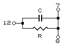
Apart from unit to unit variation, the discrimination levels will be as follows:
R = 50 k  C = 2.2 pF  :  17x
R = 20 k  C = 3.3 pF  :  23x
R =  5 k  C = 4.7 pF  :  40x
R =  2 k  C = 6.8 pF  :  88x
Intermediate values can be obtained by adjusting the value of R.
Decreasing the threshold of the A111 beyond the nominal 5 x 10 electrons can be achieved by adding a resistor from Pin 8 to ground. A 300 ohm resistor will approximately double the sensitivity resulting in a threshold of 2.5 x 10 electrons.
Revised February 8, 2001