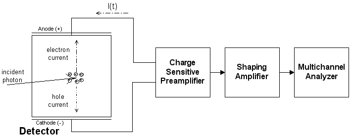
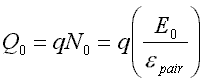
Figure 1. Schematic diagram of the detector and electronics. Typical outputs from each stage of the processing electronics are sketched below.
![[product banner]](xr100czt.gif)
The XR-100T-CZT is a high performance X-ray and g-ray detection system. It is based upon a planar Cd1-xZnxTe (CZT) semiconductor radiation detector, mounted on a thermoelectric cooler inside a small hybrid package. Thermoelectric cooling permits very high energy resolution without cryogenic cooling. This system is well-suited for X-ray and g-ray spectroscopy applications requiring high energy resolution but where the use of liquid nitrogen is inconvenient or impossible. The XR-100T-CZT is finding increasing applications in fields as diverse as chemical analyses using X-Ray Fluorescence under field conditions, isotopic measurements for environmental remediation and for national security measurements, medical uses, and many research uses.
This application note discusses the effects of charge trapping on the operation of Amptek's XR-100T-CZT radiation detectors. Charge trapping, which is not found in the more common silicon and germanium detectors, has a major impact on the performance of CZT detectors. An understanding of trapping is important to permit users and system designers to obtain the best performance for their particular applications. This note begins with a brief review of the general properties of semiconductor nuclear detectors for users who are new to this field. The note then discusses the properties of CZT which affect operational performance, particularly charge trapping. Finally, this note discusses the characteristics of the XR-100T-CZT system and its use in various applications.
All radiation detection is based on the fact that ionizing radiation, by its very definition, generates free electrons and ions (or holes) in the medium in which it interacts. The charge generated is proportional to the energy deposited: when an energy E0 is deposited, it will produce a N0=E0/epair carriers. In a semiconductor, the energy per electron-hole pair is roughly 3.4 times the bandgap. Under an applied electric field these electrons and holes will drift towards their respective oppositely charged electrodes, as sketched in Figure 1. The motion of the carriers from the point of interaction to the contact generates a transient current I(t) in the detector, and by current continuity into the electronics.
Figure 1. Schematic diagram of the detector and electronics. Typical outputs from each stage of the processing electronics are sketched below.
In most applications, one is interested in measuring the deposited energy, which is proportional to the total charge rather than the current. Charge is the integral of current so the detector is attached to a charge-sensitive preamplifer, which produces an output pulse with a voltage step directly proportional to the time integral of the current. The preamp output is then sent to a shaping amplifier, which shapes the pulse to allow accurate measurements under realistic conditions, amplifies them, and filters out noise to maximize the signal-to-noise ratio. The shaped and amplified pulse, a voltage pulse with peak amplitude proportional to the deposited energy, is then sent to a multichannel analyzer, which measures the peak ampitude of many pulses, producing a histogram showing the number of pulses with amplitude measured within the range of each channel. This is the output spectrum.
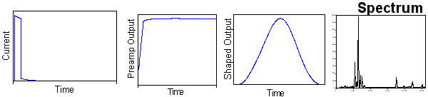
In an ideal detector, every x-ray or gamma ray photon of a given energy incident on the detector would interact and produce a voltage pulse of exactly the same amplitude. For a monoenergetic source, all of the counts would be in a single channel and the count rate would equal the rate of incident photons. This is not the case in practice. A typical real spectrum, showing the characteristic x-rays emitted by lead and measured by an XR-100T-CZT, is shown in Figure 2. Lead emits K-rays at energies of 72.8, 75, 84.9, and 87.3 keV, and L x-rays at approximately 10.5, 12.6, and 14.8 keV. In an ideal detector, the spectrum would consist of counts only at these discrete energies.
A real detector deviates from the ideal for many reasons. Some photons do not interact at all, but pass through the detector. Some of the photons which interact scatter from the detector or produce secondary emissions within the detector, depositing only a portion of the incident energy. The result is a rather complicated response function which depends on the properties of the incident radiation and on the material and size of the detector. For those events depositing full energy, various processes lead to a finite width for the peak, the energy resolution. These processes include statistical fluctuations in charge generation, trapping of carriers leading to fluctuations in the transient current, and electronic noise. The most important electronic noise sources are current and voltage fluctuations into the preamplifier input, caused by shot noise in the leakage current through the detector and thermal noise in the preamplifier input circuitry.1
In general, one would like a detector with very high sensitivity, in which the maximum number of particles interact and contribute to the full-energy peak, and with very high energy resolution, to separate closely spaced peaks and to quickly identify peaks above the background. In practice, there is a trade-off to be made between sensitivity and resolution. Practical matters, such as size, ruggedness, or the need for cryogenic cooling make further trade-offs necessary. The best energy resolution for x-rays and gamma rays is obtained using Si or Ge diode detectors, if they are cryogenically cooled to reduce leakage currents and thermal noise. The primary disadvantage of Si and Ge detectors is the need for cryogenic cooling. There are many applications where cooling the detector with liquid nitrogen is impractical, due to constant replenishment or due to the physical size and weight of the cryostat. The best sensitivity for gamma rays is obtained using scintillators, such as NaI(Tl). Scintillators are crystals in which the energy deposited produces optical photons, which are then detected by a photodetector, which produces the transient current input to the electronics. The crystals can be fabricated in very large volumes (tens of centimeters), and the light transported over large distances, resulting in excellent sensitivity. However, the resolution is limited by the fact that very few photons are detected. Photomultiplier tubes can detect the photons with high performance, but these tubes are physically large and mechanically fragile and have low sensitivity. Photodiodes can also be used but the electronic noise of the diodes further degrades the energy resolution.
There exists a variety of applications where one requires better resolution than can be achieved with scintillators, but cryogenic cooling is not practical. The ideal detector for such applications would have a bandgap much larger than that of Si or Ge, since leakage current at a given temperature decreases exponentially with the bandgap. The ideal detector would also have a high atomic number and density, because the photoelectric cross-section increases as about Z5 and the attenuation is proportional to density. This permits a much smaller detector volume for equal stopping power. 2
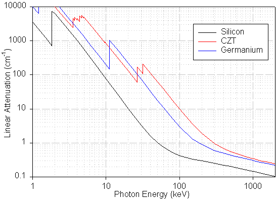
There do exist several semiconductors which meet these criteria. Unlike Si and Ge, these high-Z wide bandgap semiconductors are all compound semiconductors, made of two or more elements. The compound semiconductors most commonly used in nuclear detection applications are CdTe, its cousin Cd1-xZnxTe (CZT), and HgI2. There are many other compound semiconductors which have been studied and which have found some uses, including CdSe, PbI2, TlBr, TlBr1-xIx, InP, and others3. Figure 3 is a plot of the attenuation coefficients of Si, Ge, and CZT. CZT has dramatically higher stopping power. The probability of photoelectric versus Compton interactions is much higher at energies of common interest.
Although these compound semiconductors have certain advantages over Si and Ge, including higher attenuation coefficients and (in principal) lower bulk leakage currents due to the wider bandgap, they also have some significant disadvantages. The primary disadvantage is that they have a far higher defect density, resulting in a large number of trapping sites, leading to carrier transport properties far inferior to those of Si and Ge. Because of this, practical detector sizes are quite limited and even within the limited size, considerable spectroscopic distortion is observed. Further, leakage currents are often dominated by the defects so are not as low as might be expected from the bandgap. Other disadvantages are related to uniformity and stability of the material.
In spite of these disadvantages, compound semiconductors are the best solution for a wide variety of applications. To obtain the best performance, the user should recognize the disadvantages and how to address them. This is discussed in detail below. This section concentrates on CZT but the results are generally applicable to all of the wide-bandgap, high-Z semiconductors.
Consider again the charge transport and signal generation process sketched in Figure 1. At the electric field strengths usually found in a radiation detector, the drift velocity v of the carriers is proportional to the electric field strength E, where the constant of proportionality is defined as the mobility µ, v=µE. The instantaneous current is I=qnv, where q is the charge on an electron, n is the number of carriers, and v is their mean velocity. The duration of the transient current pulse is determined by the distance the carriers must travel. There will clearly be two distinct current pulses, one from holes and one from electrons, where the electrons will produce a much higher current for a shorter time, due to their higher mobility.
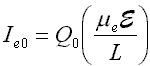
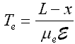
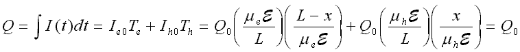
The simplest case is that of a uniform, planar detector of thickness L with a bias V, giving a constant and uniform electric field, E=V/L. Consider an X-ray which deposits energy E0 at a depth x. The interaction generates charge Q0, which gives rise to electron and hole currents Ie and Ih, which flow for a duration of Te and Th. In the absence of trapping, these quantities will be given by

The induced charge, the time integral of the current which is measured by the preamp, will be independent of depth:
Typical values for the XR-100T-CZT are epair=5.0 eV, L=0.2 cm, V=400 V, µe=1350 cm2/V-sec, and µh 120 cm2/V-sec. For a 59.5 keV gamma ray, the charge is N0=1.2x10⁴ electron-hole pairs, or Q0=1.9x10⁻¹⁵ Coulomb. The currents are Ie=26 nA, Ih=2.3 nA. The duration of the respective currents depends on the depth of interaction x. For x=1 mm, the center of the detector, we get Te = 37 nsec, Th = 415 nsec. The maximum electron transit time is obviously 74 nsec, for a pulse near the front contact where the output signal is due entirely to electrons, and similarly the maximum hole transit time is 830 nsec. The size of the voltage step at the preamplifier output is V=Q/CF, where CF is the preamplifier feedback capacitance. For the XR-100T-CZT, CF is about 50 fF, thus the preamp output setp is 40 mV for the 59.5 keV gamma ray.
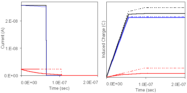
Whenever excess charge is generated in a semiconductor, thermal equilibrium is disturbed. The semiconductor returns to equilibrium via recombination, which occurs at trapping sites5. The number of free charges decays exponentially, with lifetimes te and th for the electrons and holes respectively. In Si and Ge, there are few trapping sites and the carrier lifetimes are several milliseconds long. A negligible fraction of the charges will be trapped during the charge collection process. For the compound semiconductors used in radiation detection, modern crystal growth practices lead to a much higher density of traps and hence shorter lifetimes. For CZT, typical lifetimes might be te=3x10⁻⁶ sec and th=0.05x10⁻⁶ sec. Because the hole lifetime is much shorter than the hole transit time, the induced current is significantly reduced, and further, it depends upon the depth of interaction in the detector. The time integral of the current induced into the preamplifier is called the induced charge. Figure 4 below is a plot comparing currents and induced charge for an interaction 0.25 mm into a 2 mm thick CZT detector. It should be noted that there exists a very wide variation in the hole lifetime from one detector to the next. This is not well controlled by current manufacturing practices and can easily vary over an order of magnitude.
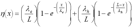
The charge collection efficiency n is defined as the total induced charge divided by the charge created, Q/Q0. It is a function of depth and is generally written in terms of the trapping length, lamdae=(µete)E and similarly for lamdah. It is given by the Hecht relation6 :
For the Amptek XR-100T-CZT with the 50 nsec hole lifetime, lamdae=2.7 cm while lamdah=0.1 cm. The electrons are nearly all collected, but clearly the holes will not be fully collected. Figure 5 is a plot showing the charge collection efficiency versus depth. For interactions near the front contact, virtually all charge is collected because the trapping time for the electrons is long compared with the transit time. For interactions near the rear contact, the induced charge is very small. Note, however, that it is non-zero. The tailing does not extend to zero amplitude.
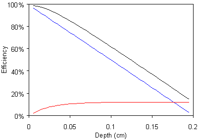
The result of trapping for spectroscopy is an effect known as "hole tailing". Consider the case where the attenuation length is long relative to detector thickness, so there is equal probability of interaction at each point in the detector. From Figure 5 above, about one-eighth of the interactions will occur near the front contact, in the region of the detector where charge collection efficiency is maximum and constant. Interactions occurring deeper will create a smaller signal. The smallest signal is half the size of the maximum. Since the plots curves down, succesively smaller signals are generated over smaller volumes and hence have fewer counts. Qualitatively, the result is a "tail" sloping down from the peak to half the peak.
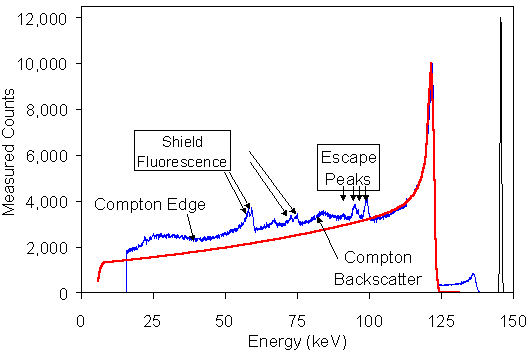
The peak shape can be quantitatively modelled as the combination of three effects: charge collection, attenuation, and electronic noise. The attenuation of the radiation yields the probability of interaction at any depth as P(x). The charge collection yields the pulse height as Q(x). Neglecting noise, the measured spectrum is the probability P of measuring a pulse height Q so will have a shape P(x(Q)). It is difficult to invert the Hecht relation so this is generally done numerically. Electronic noise will alter this shape noticably. To model this, the hole tailing spectrum must be convolved with a noise gaussian function. Figure 6 shows the complete response function computed in red. A measured 57Co spectrum is shown in blue.
The model very accurately matches the measured photopeak shape. At lower energies some deviations are observed, due largely to physical processes ignored in this model. There will be Cd, Te, and Zn escape peaks as shown. In addition, in this measurement the 57Co source was placed inside a cylindrical tungsten collimator. Photons were observed to backscatter from the collimator into the detector, producing a broad peak at 80 keV, and fluorescent x-rays were produced in the collimator and surrounding shield, at the W and Pb characteristic x-ray lines. Some of the incident gamma rays Compton scatter from the detector, with a maximum energy deposition of 40 keV. Each of these processes contribute to the spectrum, and obviously there exists hole tailing from each of these secondary peaks. A detailed discussion of these processes and there implications for spectroscopy is beyond the scope of this particular application note.
A spectrum obtained from a tail pulser, due to electronic noise alone, is shown in black. This is a gaussian, as expected, with a width of 700 eV FWHM. This width is in very good agreement with the expected electronic noise, due to the leakage current through the detector and the noise properties of the preamplifier circuitry. Note that the upper half-width at half-maximum of the measured 57Co spectrum is much larger than that of the tail pulser. This implies that there are additional gaussian broadening mechanisms affecting the CZT signal, beyond electronic noise alone. To obtain the model spectrum shown in Figure 6, a gaussian broadening of 1.1 keV FWHM was required.
The existing state-of-the art of crystal growth produces considerable macroscopic non-uniformity in the crystals of compound semiconductors. A single boule will often contain several crystalline regions, with different orientations and obviously a high density of crystal defects along the boundary. If a radiation detector is cut from a region containing two crystals, there will be many defects and hence a short lifetime. Moreover, the conductivity is usually larger along a grain boundary, which alters the applied electric field. In a polycrystalline detector, the electric field will not be uniform and constant. There are other macroscopic defects which can alter the charge collection properties. For example, it is possible for Te inclusions to form. This leads to a small metallic region, which obviously alters the internal electric field.
Even in the absence of macroscopic defects, it is common to observe variations in the material properties over the volume of a detector. For example, the Cd to Zn ratio can vary radially in the grown crystal, due to thermal gradients. This causes the bandgap to vary over the volume of a detector, and hence the charge per pair, causing an obvious peak broadening. Spatial variations in the trap density cause spatial variations in the lifetime and hence in the tailing. One region of the detector might produce much worse tailing than another.
The result of a non-uniform electric field or non-uniform trapping lifetimes will be to alter the detailed shape of the hole tailing. The general properties of the tail will remain, but the detailed shape will not match that given by the Hecht equation and shown in Figure 6.
When carriers are trapped, they either recombine or are subsequently detrapped and contribute to a delayed current. In most cases, the detrapping lifetime is much longer than the integration time of the electronics so the detrapping does not contribute to the primary signal but creates an essentially DC current. However, while the charges are trapped they alter slightly the internal electric field inside the detector. Since the electrons and holes are separated, the internal field is reduced, an effect known as polarization. If a detector is initially unbiased, when bias is applied some carriers will move and the internal field will be reduced. In the past, this was a major problem with compound semiconductors, with the internal field decreasing over time periods of seconds to days. Modern crystal growth and fabrication practices make this rare today. In an extremely large radiation flux, it is possible to fill enough deep traps to alter the internal field. In such cases, heating of the crystal will accelerate the detrapping process.
There are some very important conclusions we can make regarding general properties of hole tailing.
It is important to note that there does not exist a universally accepted method for including the effects of hole tailing in describing the performance of wide bandgap semiconductors. Different manufacturers quantify performance differently. Some present only the FWHM of the peak at some energy, which mixes electronic noise and hole tailing. Some present only the upper half-width at half maximum, and some refer to twice this as the "FWHM". This is only electronic noise so does not at all address hole tailing. A very useful set of parameters was proposed7 , but has not been adopted by the industry.
Given that charge transport is a major problem in CZT, and in other wide bandgap semiconductors, four primary solutions have been used to improve spectroscopic performance.
The ideal solution would be to learn how to grow crystals without defects. A great deal of research has gone into this, and is still going into this, and significant improvements have been made8 . The hole µt in CZT have increased several-fold over the past few years and will probably continue to improve. Each boule now contains larger single crystals, and the spatial variations in material have decreased. Continued improvements are likely, but it seems extremely unlikely that CZT will approach the characteristics of Si and Ge any time soon.
It is inherently more difficuly to grow a defect-free compound semiconductor, with two or more constituents, than one made from a single element. In the compound semiconductor, each atom in the lattice must be in the correct place. A slight excess of the atoms of one element at the lattice location where the crystal is growing will lead to defects. So while trapping lengths and uniformity will improve, allowing growth of large crystals, hole tailing is likely to be important for quite a while. A variety of other solutions have therefore been explored.
One obvious means of improving charge collection is to apply a higher electric field, but this results in increased leakage currents and therefore increased electronic noise. What this means is that the optimum bias voltage depends upon the details of a user's application. For the detection of x-rays, which stop near the front contact and for which hole tailing is unimportant, a reduced bias voltage will often improve performance by reducing electronic noise. For the detection of gamma rays, if one requires high efficiency and does not need the ultimate in resolution, then an increased bias voltage will help.
Cooling the crystal will reduce the leakage currents, permitting a higher bias voltage with no loss of resolution. For CZT, which has a fairly low leakage current at room temperature, only slight cooling provides significant improvements. A single stage thermoelectric cooler can generate a temperature differential of 50�C, reducing the leakage current by a factor of approximately 100. Alternately, the bias voltage can be increased greatly with little impact on noise. Thermoelectric cooling has major advantages over the cryogenic cooling required for Si and Ge. The cooling is fast (tens of seconds) and, from the user's perspective, all that must be done is to apply power. Thermoelectric cooling is invisible to the user, so the system still operates as if it were at room temperature. Amptek's XR-100T-CZT system operates using thermoelectric cooling9.
Most CZT detectors are based on the M-S-M structure, in which symmetric metal contacts are placed on a wafer of the semiconductor. The resulting device is symmetric, with no forward or reverse direction. It is also essentially ohmic: the device is fully depleted at a low bias voltage, and for all bias voltages above this the dark current increases linearly with voltage. It is possible to fabricate a diode structure with CZT and reverse bias it, to reduce the leakage current. Various diode structures have been used, including blocking contacts (M-pi-N), doping (P-I-N), and heterojunctions10. The M-pi-N devices demonstrated very good resolution but had significant problems with polarization. Both these and the heterojunction devices have yet to reach manufacturing. The PIN devices are beginning to show up in commercial applications.
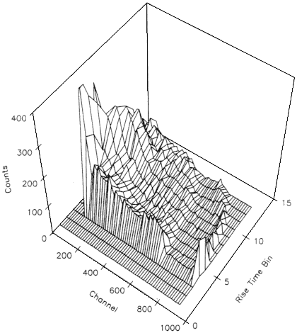
As should be clear from the previous discussion, the charge collection efficiency of a CZT detector depends upon the depth of the point of interaction. Because of the difference in carrier mobility, the risetime of the preamplifier signal also depends upon the depth of interaction: in interactions close to the front contact, most of the signal is due to the electrons, which travel quickly across the detector. Since both risetime and charge collection efficiency are correlated with depth of interaction, the risetime is therefore correlated with depth of interaction. One can use measurements of the risetime to deduce charge collection efficiency and thus improve spectroscopic performance. Methods based on measuring both risetime and induced charge are termed biparametric methods.
Figure 7 shows a measured biparametric spectrum from a 2x2x2 mm3 CdTe detector, showing counts versus pulse height and risetime of the shaped output11 . The maximum pulse heights are observed at the shortest risetimes and are most probable. With increasing risetime, the pulse height decreases and the probability decreases. This is seen very clearly as the channel associated with the 662 keV peak curves towards lower values.
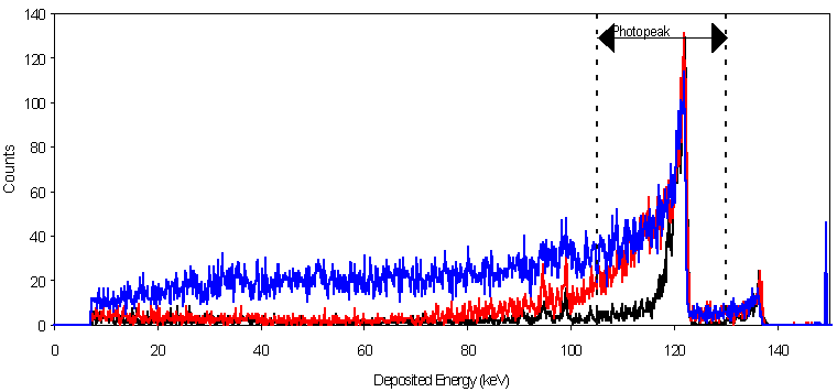
Risetime discrimination (RTD) is one method which has long been used to improve spectral shape using risetime information12 . In this method, all pulses with a risetime exceeding some threshold are rejected, thus all pulses which would contribute to the tail are rejected. Amptek offers RTD with XR-100T-CZT detectors to provide very high resolution. This technique is effective at improving the resolution but leads to significantly reduced sensitivity since many counts are rejected. As can be seen in Figure 5 above, only the top 25% or so of the detector has nearly uniform charge collection. RTD applied to this detector would lead to an effective depth of only 0.5 mm, since the counts in the rest of the volume are rejected.
Some trade-off between resolution and sensitivity is possible: opening the risetime window accepts more counts but these are located in the tail. This is shown clearly in Figure 8. It should be noted that RTD does not reduce the photopeak sensitivity: the same number of counts will go into the main photopeak with RTD on and off. What RTD does is to reject those that would appear in the tail, which often interfere with lower energy peaks. The "photopeak" region denoted in this plot is a "standardized" region that has been used to compare the performance of many wide bandgap, high-Z semiconductors13.
Risetime compenstation is an alternate biparametric method in which both the induced charge and the risetime are measured and then, from the risetime, the charge collection efficiency is deduced. The measured induced charge is multiplied by an appropriate correction factor, yielding a corrected pulse amplitude14 . This is a very powerful technique, permitting very high resolution with no loss of sensitive volume. However, there are certain disadvantages. First, the electronics required to measure the risetime and apply any compensation are rather complicated. Second, as can be seen in Figure 7, the pulse heigh deficit depends non-linearly on risetime. Some commercial devices apply a linear correction, but this is obviously valid only over a limited depth of the detector. Research systems have been developed to apply non-linear corrections which use the entire depth of the detector, but because of their complexity and the difficulty of doing a non-linear calibration on each detector, these systems have not made it into commercial use.
Biparametric techniques have a fundamental limitation in that they are only applicable to pure photoelectric interactions. If an incident photon undergoes a photoelectric interaction, it deposits all its energy at a single point, for which there are two well-defined parameters, risetime and charge loss. If a photon undergoes first a Compton scatter and then photoelectric absorption, then energy is deposited at two depths in the crystal and there are four parameters, a risetime and a charge loss for each interaction point. The deduced charge loss does not precisely equal the charge loss for either depth or the mean charge loss, so some loss of resolution results. For 662 keV photons interacting in a 2 mm CZT detector, the number of photons undergoing a pure photoelectric interaction is comparable to the number first undergoing a Compton scatter and then a photoelectric absorption.
It was noted before that the electrons are nearly fully collected for interactions occuring throughout the detector volume and that hole tailing is due only to the signal due to holes. If one could measure the current due only to the electrons, and neglect that due to the holes, then the measured charge would not depend on depth. This was done long ago for ion chambers, by locating a grid between the anode and cathode. Only the current due to electron drift between the grid and the anode is measured, resulting in a signal due only to electrons15 . It is quite difficult to fabricate a grid inside a semiconductor detector. In recent years, a variety of techniques have been developed in which the contacts on the surface of the detector are patterned and read out in such a way that the output signal is due only to electrons. These techniques include hemispherical detectors15, coplanar anodes17, small pixel detectors18, a geometrically weighted grid19, the SpectrumPlus design20, and a variety of others. The development of detectors using these contacts is a very active and promising field of research, for large volume CZT detectors used in gamma ray detection.
Application Note ANCZT-2 Rev. 1 written by Bob Redus
References
Volume editors Schlesinger & James
Revised February 8, 2001